I've been learning a lot about transistors, lately. This is because I found myself having to switch a load that would be too large for an IO pin. Here I summerize my newly gathered knowledge on them.
A BJT transistor is switched ON/OFF using current at the base. This current is then multiplied at Collector/Emitter.
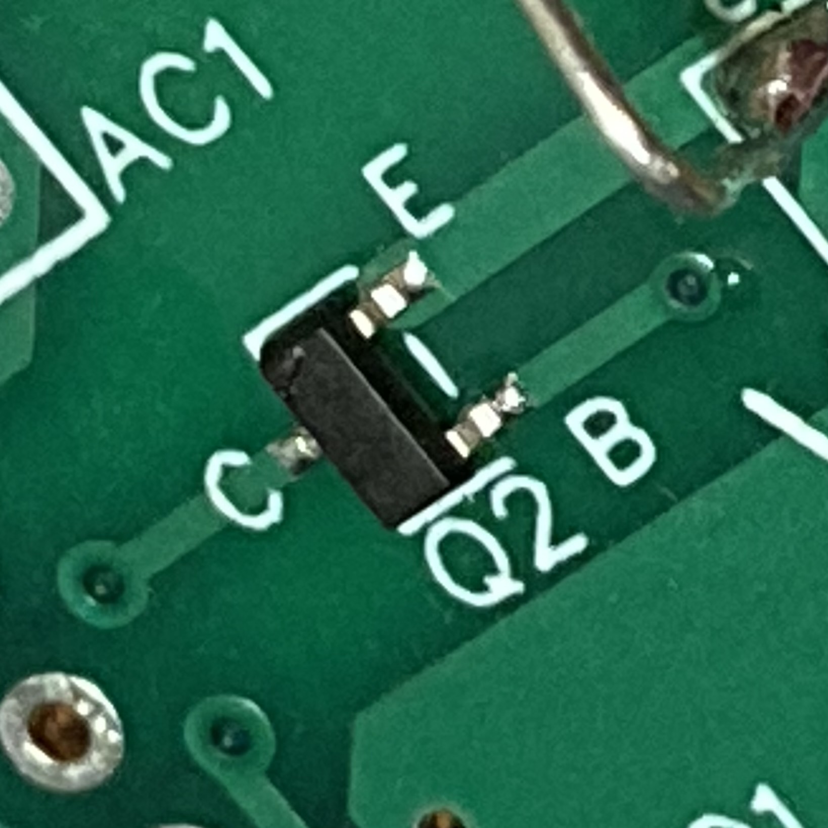
To tune the current flowing through the base, we need a bias resistor. This makes PCB design bulkier, but you can get pre-biased transistors. I find I need to get them with a low Ohm bias, else my transistor will not switch fully on.
BJT comes in two variants, NPN and PNP. The schematic symbol differs in which way the arrow points. Mnemonic: NPN has the arrow "Not Pointing iN."
PNP transistors can be used to switch a load at its high-side: You cut the load's connection to V+ ON/OFF.
NPN transistors can be used to switch a load at its low-side: You cut the load's connection to GND ON/OFF.
MOSFET transistors are often a better choice, unlike of BJT's current based switching, the switch based on voltage at the gate.
MOSFET comes in two variants, P-CHANNEL and N-CHANNEL.
P-CHANNEL transistors can be used to switch a load at its high-side: You cut the load's connection to V+ ON/OFF. A 0V at the gate will switch on the transistor. Source is connected to V+ and Drain is connected to the load.
N-CHANNEL transistors can be used to switch a load at its low-side: You cut the load's connection to GND ON/OFF. A V+ at the gate will switch on the transistor. Source is connected to GROUND and Drain is connected to the load.
To simplify a PCB design, you can get two transistors that share its housing in an "Array."